

约翰·特纳斯面临的首个重大问题是人工智能
The Verge
·
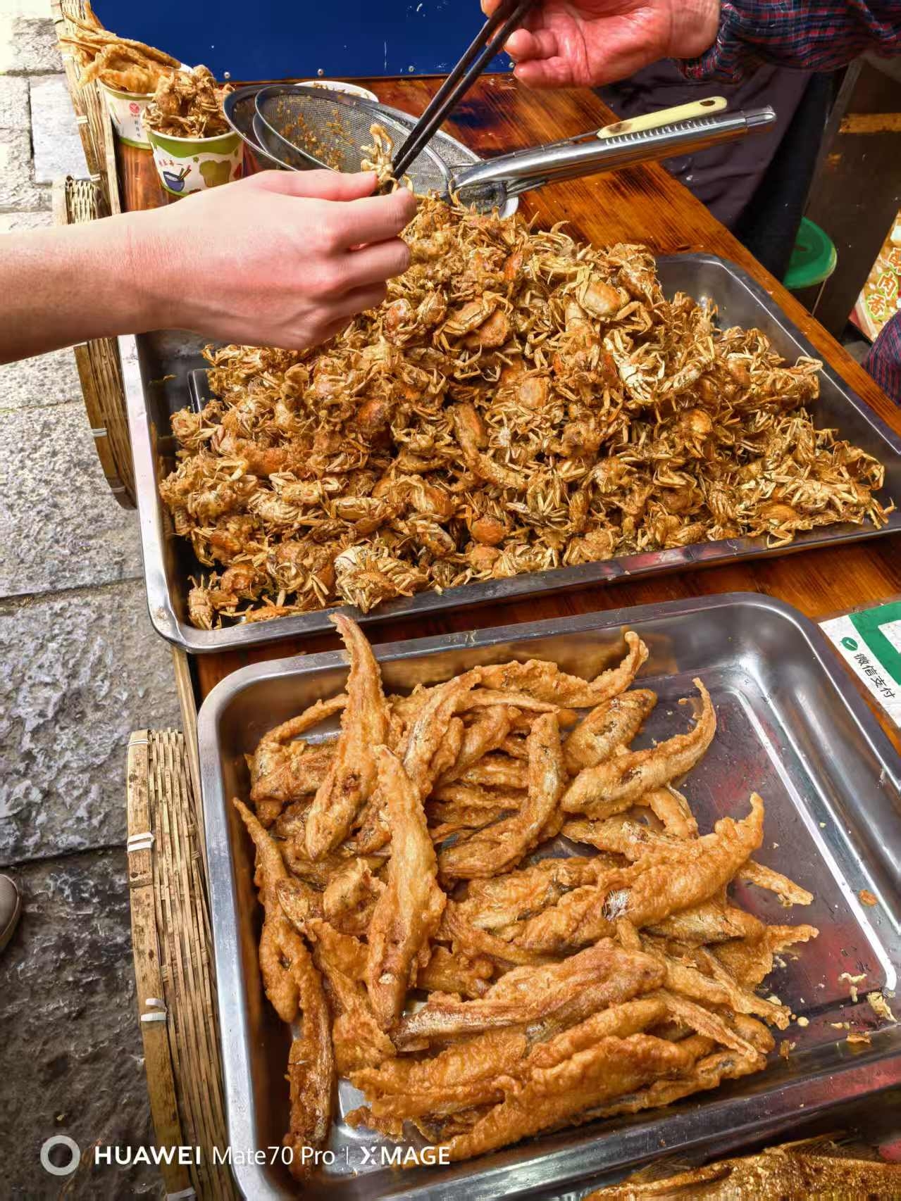
再也不会去的“窑湾古镇”
老张博客
·
JetBrains推出的Kotlin专业证书 – 现已在LinkedIn Learning上线
The JetBrains Blog
·
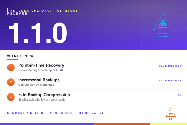
Percona Operator for MySQL 1.1.0:时间点恢复、增量备份与压缩
Percona Database Performance Blog
·


《Splatoon Raiders》将于7月在Switch 2上发布
The Verge
·


SpaceX的首次公开募股是对太空未来的万亿美元赌注
The Verge
·
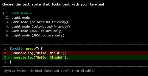
国内环境下的Claude Code安装与使用教程
程序新视界
·
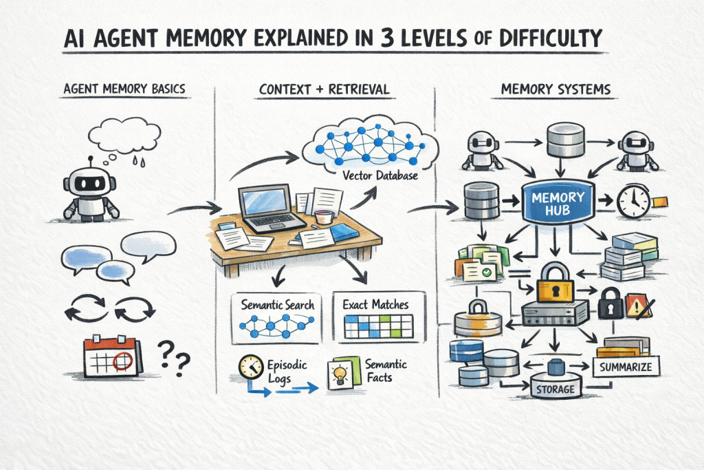
人工智能代理记忆机制的三种难度解析
MachineLearningMastery.com
·

